- 您现在的位置:买卖IC网 > Sheet目录983 > HI5828EVAL2 (Intersil)EVALUATION PLATFORM HI5828
�� �
�
�Application� Note� 9855�
�Appendix� A� Description� of� Architecture�
�The� segmented� current� source� architecture� has� the� ability� to�
�improve� the� converter’s� performance� by� reducing� the� amount�
�of� current� that� is� switching� at� any� one� time.� In� a� segmented�
�current� source� arrangement,� transitions� such� as� midscale�
�become� one� in� which� you� simply� have� an� additional�
�intermediate� current� source� turning� on� and� several� minor�
�ones� turning� off.� In� the� case� of� the� HI5760� 10-Bit� DAC,� there�
�are� 31� intermediate� current� segments� that� represent� the� 5�
�MSBs� and� five,� binary-weighted� current� sources� representing�
�each� of� the� five� LSBs.� See� the� Functional� Block� Diagram� in�
�the� datasheet� for� a� visual� representation.� To� relate� the�
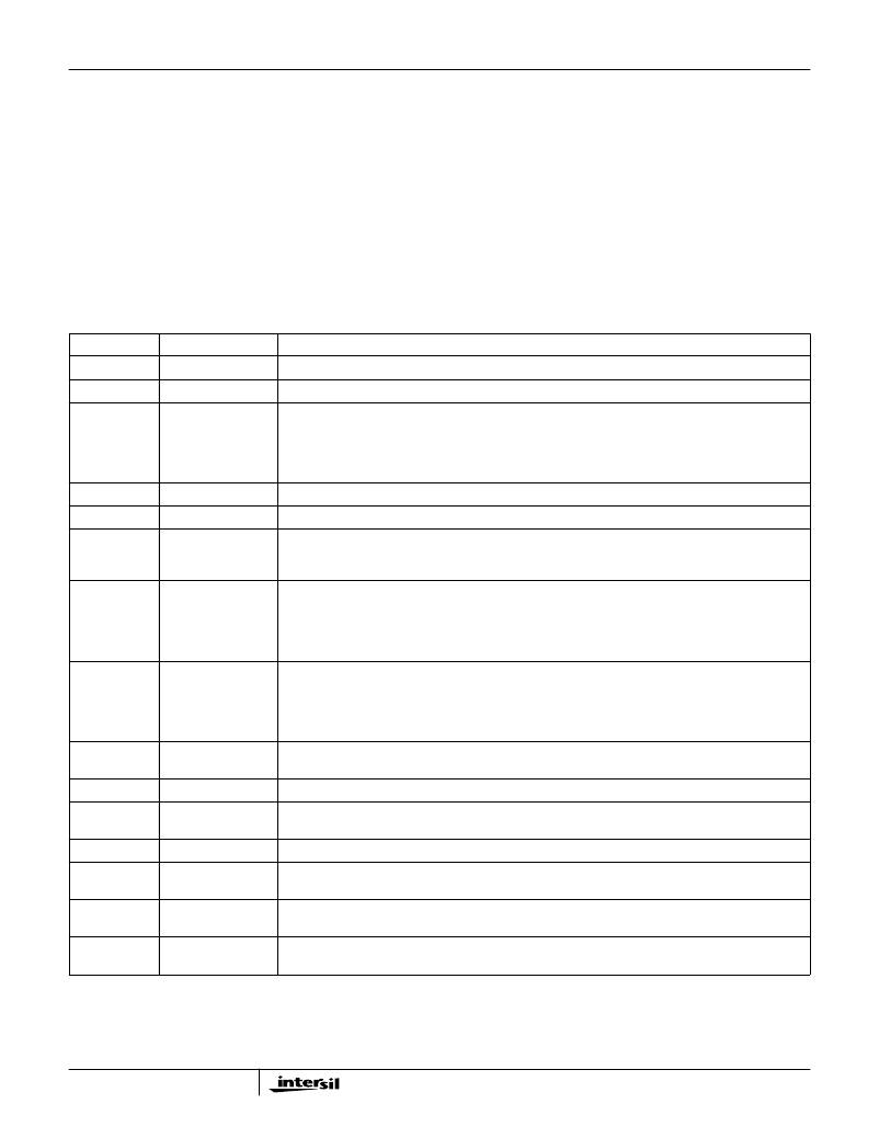
�HI5828� Pin� Descriptions�
�midscale� transition� example� to� the� HI5760,� consider� the�
�following:� The� code� 0111111111� would� be� represented� by� 15�
�intermediate� current� segments� and� each� of� the� 5� LSB� current�
�sources� all� turned� on.� To� transition� to� code� 1000000000� would�
�simply� require� turning� off� the� 5� LSB� current� sources� and�
�turning� on� the� next� intermediate� current� segment,� bringing� the�
�total� amount� of� current� switching� at� this� ‘major’� code� transition�
�equal� to� the� same� amount� switching� at� 30� other� code�
�transition� points� in� the� code� ramp� from� 0� to� 1023,� so� that� the�
�total� glitch� energy� is� distributed� more� evenly.� The� HI5828� uses�
�this� technique� but� with� a� 5� MSB/7� LSB� split.�
�PIN� NO.�
�11,� 19,� 26�
�13,� 24�
�28�
�27�
�10�
�20�
�14,� 23�
�12,� 25�
�NAME�
�AGND�
�A� VDD�
�CLK�
�DGND�
�D� VDD�
�FSADJ�
�ICOMP1,� QCOMP1�
�ICOMP2,� QCOMP2�
�DESCRIPTION�
�Analog� Ground.�
�Analog� Supply� (+3V� to� +5V).�
�Clock� Input.� The� master� and� slave� latches� shown� in� the� functional� block� diagram� are� simple� D-latches.�
�Input� data� to� the� DAC� passes� through� the� “master”� latches� when� the� clock� is� low� and� is� latched� into� the�
�“master”� latches� when� the� clock� is� high.� Data� presented� to� the� “slave”� latch� inputs� passes� through� when�
�the� clock� is� high� and� is� latched� into� the� “slave”� latches� when� the� clock� is� low.� This� master-slave�
�arrangement� comprises� an� edge-triggered� flip-flop,� with� the� DAC� being� updated� on� the� rising� clock� edge.�
�Connect� to� Digital� Ground.�
�Digital� Supply� (+3V� to� +5V).�
�Full� Scale� Current� Adjust.� Use� a� resistor� to� ground� to� adjust� full� scale� output� current.� Full� Scale� Output�
�Current� =� 32� x� V� FSADJ� /R� SET� .� Where� V� FSADJ� is� the� voltage� at� this� pin.� V� FSADJ� tracks� the� voltage� on� the�
�REFIO� pin� (refer� to� the� functional� block� diagram);� which� is� typically� 1.2V� if� the� internal� reference� is� used.�
�Compensation� Pin� for� Use� in� Reducing� Bandwidth/Noise.� Each� pin� should� be� individually� decoupled� to�
�AVDD� with� a� 0.1� μ� F� capacitor.� To� minimize� crosstalk,� the� part� was� designed� so� that� these� pins� must� be�
�connected� externally,� ideally� directly� under� the� device� packaging.� The� voltage� on� these� pins� is� used� to�
�drive� the� gates� of� the� PMOS� devices� that� make� up� the� current� cells.� Only� the� ICOMP1� pin� is� driven� and�
�therefore� QCOMP1� needs� to� be� connected� to� ICOMP1,� but� de-coupled� separately� to� minimize� crosstalk.�
�Compensation� Pin� for� Internal� Bias� Generation.� Each� pin� should� be� individually� decoupled� to� AGND� with�
�a� 0.1� μ� F� capacitor.� The� voltage� generated� at� these� pins� represents� the� voltage� used� to� supply� power� to�
�the� switch� drivers� (refer� to� the� functional� block� diagram)� which� is� 2.0V� nominal.� This� arrangement� helps�
�to� minimize� clock� feedthrough� to� the� current� cell� transistors� for� reduced� glitch� energy� and� improved�
�spectral� performance.�
�43-48,� 1-6,�
�29-40�
�ID11-ID0,� QD11-QD0� Digital� Data� Input� Ports.� Bit� 11� is� Most� Significant� Bit� (MSB)� and� bit� 0� is� the� Least� Significant� Bit� (LSB).�
�15,� 22�
�16,� 21�
�7,� 8,� 41,� 42�
�17�
�18�
�9�
�IOUTA,� QOUTA�
�IOUTB,� QOUTB�
�NC�
�REFIO�
�REFLO�
�SLEEP�
�Current� Outputs� of� the� Device.� Full� scale� output� current� is� achieved� when� all� input� bits� are� set� to� binary� 1.�
�Complementary� Current� Outputs� of� the� Device.� Full� scale� output� current� is� achieved� on� the�
�complementary� outputs� when� all� input� bits� are� set� to� binary� 0.�
�No� Connection.�
�Reference� voltage� input� if� Internal� reference� is� disabled.� Use� 0.1� μ� F� cap� to� ground� when� internal� reference�
�is� enabled.�
�Reference� Low� Select.� To� enable� the� internal� reference,� connect� REFLO� to� analog� ground.� To� disable�
�the� internal� reference� circuitry� this� pin� should� be� connected� to� A� VDD� .�
�Control� Pin� for� Power-Down� Mode.� Sleep� Mode� is� active� high;� connect� to� ground� for� Normal� Mode.� Sleep�
�pin� has� internal� 20� μ� A� (nominal)� active� pull-down� current.�
�3-4�
�发布紧急采购,3分钟左右您将得到回复。
相关PDF资料
HI5960SOICEVAL1
EVALUATION PLATFORM SOIC HI5960
HI7188EVAL
EVALUATION PLATFORM HI7188
HI7190EVAL
EVALUATION PLATFORM HI7190
HJ4-L-DC12V
RELAY GEN PURPOSE 4PDT 5A 12V
HL2-HP-AC100V-F
RELAY GEN PURPOSE DPDT 10A 100V
HLM01510Z16K50JJ
RES 16.5K OHM 15W 5% WW
HMC1043-DEMO
DEMONSTRATION BOARD FOR HMC1043
20021311-00034T1LF
集管和线壳 RCPT VT TH
相关代理商/技术参数
HI5828IN
功能描述:DAC DUAL 12BIT 130MHZ 48-LQFP RoHS:否 类别:集成电路 (IC) >> 数据采集 - 数模转换器 系列:- 标准包装:2,400 系列:- 设置时间:- 位数:18 数据接口:串行 转换器数目:3 电压电源:模拟和数字 功率耗散(最大):- 工作温度:-40°C ~ 85°C 安装类型:表面贴装 封装/外壳:36-TFBGA 供应商设备封装:36-TFBGA 包装:带卷 (TR) 输出数目和类型:* 采样率(每秒):*
HI5860
制造商:INTERSIL 制造商全称:Intersil Corporation 功能描述:12-Bit, 125MSPS, CommLinkTM High Speed D/A Converter
HI5860 WAF
制造商:Intersil Corporation 功能描述:
HI5860_05
制造商:INTERSIL 制造商全称:Intersil Corporation 功能描述:12-Bit, 130MSPS, High Speed D/A Converter
HI5860_08
制造商:INTERSIL 制造商全称:Intersil Corporation 功能描述:12-Bit, 130MSPS, High Speed D/A Converter
HI5860IA
功能描述:CONV D/A 12BIT 130MSPS 28-TSSOP RoHS:否 类别:集成电路 (IC) >> 数据采集 - 数模转换器 系列:- 标准包装:2,400 系列:- 设置时间:- 位数:18 数据接口:串行 转换器数目:3 电压电源:模拟和数字 功率耗散(最大):- 工作温度:-40°C ~ 85°C 安装类型:表面贴装 封装/外壳:36-TFBGA 供应商设备封装:36-TFBGA 包装:带卷 (TR) 输出数目和类型:* 采样率(每秒):*
HI5860IA-T
功能描述:CONV D/A 12BIT 130MSPS 28-TSSOP RoHS:否 类别:集成电路 (IC) >> 数据采集 - 数模转换器 系列:- 标准包装:2,400 系列:- 设置时间:- 位数:18 数据接口:串行 转换器数目:3 电压电源:模拟和数字 功率耗散(最大):- 工作温度:-40°C ~ 85°C 安装类型:表面贴装 封装/外壳:36-TFBGA 供应商设备封装:36-TFBGA 包装:带卷 (TR) 输出数目和类型:* 采样率(每秒):*
HI5860IB
功能描述:CONV D/A 12-BIT 130MSPS 28-SOIC RoHS:否 类别:集成电路 (IC) >> 数据采集 - 数模转换器 系列:- 标准包装:2,400 系列:- 设置时间:- 位数:18 数据接口:串行 转换器数目:3 电压电源:模拟和数字 功率耗散(最大):- 工作温度:-40°C ~ 85°C 安装类型:表面贴装 封装/外壳:36-TFBGA 供应商设备封装:36-TFBGA 包装:带卷 (TR) 输出数目和类型:* 采样率(每秒):*